Breakthrough Device can Split Signals on Terahertz Wavelengths

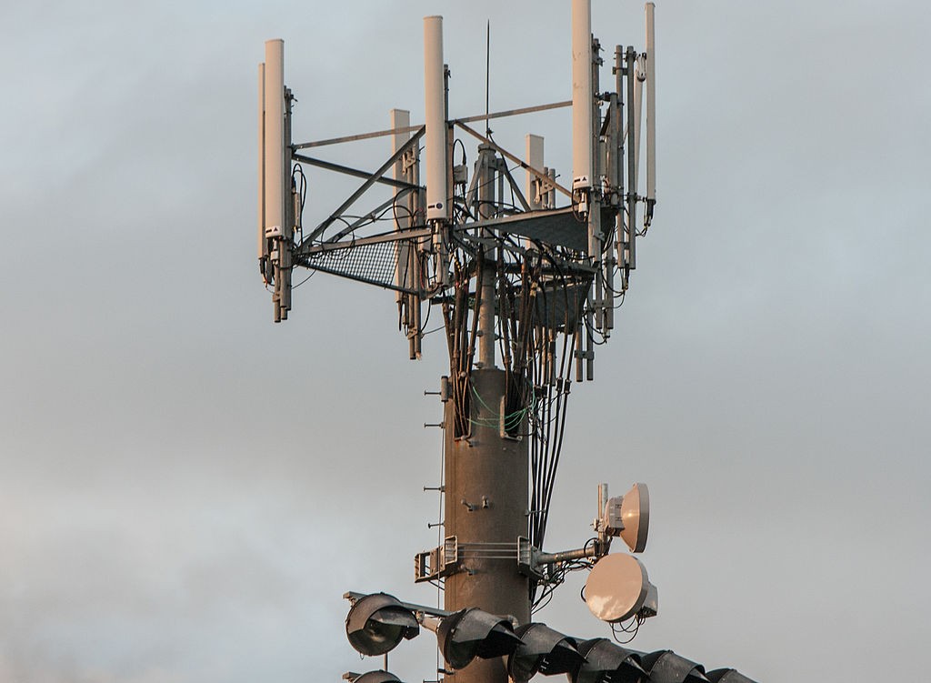
One of the most basic components of any communications network is a power splitter that allows a signal to be sent to multiple users and devices. Researchers have now developed just such a device for terahertz radiation—a range of frequencies that may one day enable data transfer up to 100 times faster than current cellular and Wi-Fi networks.

“One of the big thrusts in terahertz technology is wireless communications,” says Kimberly Reichel, a postdoctoral researcher in Brown University’s School of Engineering who led the device’s development. “We believe this is the first demonstration of a variable broadbrand power splitter for terahertz, which would be a fundamental device for use in a terahertz network.”

The device could have numerous applications, including as a component in terahertz routers that would send data packets to multiple computers, just like the routers in current Wi-Fi networks.

Today’s cellular and Wi-Fi networks rely on microwaves, but the amount of data that can travel on microwaves is limited by frequency. Terahertz waves (which span from about 100 to 10,000 GHz on the electromagnetic spectrum) have a higher frequency and therefore the potential to carry much more data. Until recently, however, terahertz hasn’t received much attention from scientists and researchers, so many of the basic components for a terahertz communications network simply don’t exist.

Daniel Mittleman, a professor in Brown’s School of Engineering, has been working to develop some of those key components. His lab recently developed the first system for terahertz multiplexing and demultiplexing—a method of sending multiple signals through a single medium and then separating them back out on the other side. Mittleman’s lab has also produced a new type of lens for focusing terahertz waves.

Each of the components Mittleman has developed makes use of parallel-plate waveguides—metal sheets that can constrain terahertz waves and guide them in particular directions.

“We’re developing a family of waveguide tools that could be integrated to create the appropriate signal processing that one would need to do networking,” says Mittleman, who was a coauthor of the new paper along with Reichel and Brown research professor Rajind Mendis. “The power splitter is another member of that family.”

The new device consists of several waveguides arranged to form a T-junction. Signal going into the leg of the T is split by a triangular septum at the junction, sending a portion of the signal down each of the two arms. The septum’s triangular shape minimizes the amount of radiation that reflects back down the leg of the T, reducing signal loss. The septum can be moved right or left in order to vary the amount of power that is sent down either arm.

“We can go from an equal 50/50 split up to a 95/5 split, which is quite a range,” Reichel says.

For this proof-of-concept device, the septum is manipulated manually, but Mittleman says that process could easily be motorized to enable dynamic switching of power output to each channel. That could enable the device to be incorporated in a terahertz router.

“It’s reasonable to think that we could operate this at sub-millisecond timescales, which would be fast enough to do data packet switching,” Mittleman says. “So this is a component that could be used to enable routing in the manner of the microwave routers we use today.”

The researchers plan to continue to work with the new device. A next step, they say, would be to start testing error rates in data streams sent through the device.

“The goal of this work was to demonstrate that you can do variable power switching with a parallel-plate waveguide architecture,” Mittleman says. “We wanted to demonstrate the basic physics and then refine the design.”

The National Science Foundation and the W. M. Keck Foundation funded the work. The new device is described in the journal Scientific Reports.

Source: Republished from Futurity.org as a derivative work under the Attribution 4.0 International license. Original article posted to Futurity by .
Featured Image Credit: Tony Webster, via Wikimedia Commons

Now, Check Out:

American Medical Association warns of health and safety problems from ‘white’ LED streetlights

By Richard G. ‘Bugs’ Stevens, University of Connecticut.

The American Medical Association (AMA) has just adopted an official policy statement about street lighting: cool it and dim it.

The statement, adopted unanimously at the AMA’s annual meeting in Chicago on June 14, comes in response to the rise of new LED street lighting sweeping the country. An AMA committee issued guidelines on how communities can choose LED streetlights to “minimize potential harmful human health and environmental effects.”

Municipalities are replacing existing streetlights with efficient and long-lasting LEDs to save money on energy and maintenance. Although the streetlights are delivering these benefits, the AMA’s stance reflects how important proper design of new technologies is and the close connection between light and human health.

Light is composed of light of different colors (red, blue and green) and some LED streetlights have a relatively high portion of blue light, which can disrupt people’s circadian rhythms. flakepardigm/flickr, CC BY-SA

The AMA’s statement recommends that outdoor lighting at night, particularly street lighting, should have a color temperature of no greater than 3000 Kelvin (K). Color temperature (CT) is a measure of the spectral content of light from a source; how much blue, green, yellow and red there is in it. A higher CT rating generally means greater blue content, and the whiter the light appears.

A white LED at CT 4000K or 5000K contains a high level of short-wavelength blue light; this has been the choice for a number of cities that have recently retrofitted their street lighting such as Seattle and New York.

But in the wake of these installations have been complaints about the harshness of these lights. An extreme example is the city of Davis, California, where the residents demanded a complete replacement of these high color temperature LED street lights.

Can communities have more efficient lighting without causing health and safety problems?

Two problems with LED street lighting

An incandescent bulb has a color temperature of 2400K, which means it contains far less blue and far more yellow and red wavelengths. Before electric light, we burned wood and candles at night; this artificial light has a CT of about 1800K, quite yellow/red and almost no blue. What we have now is very different.

The new “white” LED street lighting which is rapidly being retrofitted in cities throughout the country has two problems, according to the AMA. The first is discomfort and glare. Because LED light is so concentrated and has high blue content, it can cause severe glare, resulting in pupillary constriction in the eyes. Blue light scatters more in the human eye than the longer wavelengths of yellow and red, and sufficient levels can damage the retina. This can cause problems seeing clearly for safe driving or walking at night.

You can sense this easily if you look directly into one of the control lights on your new washing machine or other appliance: it is very difficult to do because it hurts. Street lighting can have this same effect, especially if its blue content is high and there is not appropriate shielding.

The other issue addressed by the AMA statement is the impact on human circadian rhythmicity.

Color temperature reliably predicts spectral content of light – that is, how much of each wavelength is present. It’s designed specifically for light that comes off the tungsten filament of an incandescent bulb.

However, the CT rating does not reliably measure color from fluorescent and LED lights.

Another system for measuring light color for these sources is called correlated color temperature (CCT). It adjusts the spectral content of the light source to the color sensitivity of human vision. Using this rating, two different 3000K light sources could have fairly large differences in blue light content.

Therefore, the AMA’s recommendation for CCT below 3000K is not quite enough to be sure that blue light is minimized. The actual spectral irradiance of the LED – the relative amounts of each of the colors produced – should be considered, as well.

The reason lighting matters

The AMA policy statement is particularly timely because the new World Atlas of Artificial Night Sky Brightness just appeared last week, and street lighting is an important component of light pollution. According to the AMA statement, one of the considerations of lighting the night is its impact on human health.

In previous articles for The Conversation, I have described how lighting affects our normal circadian physiology, how this could lead to some serious health consequences and most recently how lighting the night affects sleep.

LEDs (the yellow device) produce a highly concentrated light, which makes glare a problem for LED streetlights since it can hamper vision at night.
razor512/flickr, CC BY

In the case of white LED light, it is estimated to be five times more effective at suppressing melatonin at night than the high pressure sodium lamps (given the same light output) which have been the mainstay of street lighting for decades. Melatonin suppression is a marker of circadian disruption, which includes disrupted sleep.

Bright electric lighting can also adversely affect wildlife by, for example, disturbing migratory patterns of birds and some aquatic animals which nest on shore.

Street lighting and human health

The AMA has made three recommendations in its new policy statement:

First, the AMA supports a “proper conversion to community based Light Emitting Diode (LED) lighting, which reduces energy consumption and decreases the use of fossil fuels.”

Second, the AMA “encourage[s] minimizing and controlling blue-rich environmental lighting by using the lowest emission of blue light possible to reduce glare.”

Third, the AMA “encourage[s] the use of 3000K or lower lighting for outdoor installations such as roadways. All LED lighting should be properly shielded to minimize glare and detrimental human and environmental effects, and consideration should be given to utilize the ability of LED lighting to be dimmed for off-peak time periods.”

There is almost never a completely satisfactory solution to a complex problem. We must have lighting at night, not only in our homes and businesses, but also outdoors on our streets. The need for energy efficiency is serious, but so too is minimizing human risk from bad lighting, both due to glare and to circadian disruption. LED technology can optimize both when properly designed.

The ConversationRichard G. ‘Bugs’ Stevens, Professor, School of Medicine, University of Connecticut

This article was originally published on The Conversation. Read the original article.

Now, Check Out:

Why kids are key to unlocking the potential of 3D printing

Carolyn Conner Seepersad, University of Texas at Austin

Mattel recently announced that it will release a US$300 3D printer for kids in time for the 2016 holiday season. With accompanying software that is specially tailored for young toy designers, the ThingMaker promises to introduce a new generation of innovators to the up-and-coming world of 3D printing.

Known in technology circles as “additive manufacturing,” 3D printing has grown into a $4 billion industry since it was first commercialized 30 years ago by 3D Systems. For most of its history, though, it has been out of the reach of typical consumers. Most industrial-scale 3D printing machines cost tens or hundreds of thousands of dollars and fabricate parts with materials that cost orders of magnitude more than those used in most consumer products.

Over the past 10 years, however, inexpensive personal 3D printers became more popular, starting with the wildly popular RepRap project in the U.K. and Fab@Home in the U.S. More than 100,000 desktop 3D printers were sold in the U.S. in 2014 alone, almost double the number sold the previous year. Even though these desktop machines are affordable and widely available, they aren’t always kid-friendly. Hot nozzles and plates and a variety of moving parts are exposed to the user, and maintenance often involves such consumer-unfriendly tasks as disassembling a clogged nozzle mechanism and leveling build plates by hand with precision screws.

If a machine like Mattel’s ThingMaker can avoid the downsides of other 3D printers and be truly kid-friendly, what impact might it have on our kids, the next generation of innovators?

Improving access to innovation

For more than a year, my research group at the University of Texas at Austin has been running the Innovation Station, a 3D printing vending machine that we designed and built to provide open access to 3D printing on the university campus. After fabricating more than 1,000 parts, it gives us a unique window into the types of objects young people will fabricate when 3D printing is freely available to them.

Checking out the new dimension: college students contemplate the possibilities presented by the Innovation Station. Cockrell School of Engineering at The University of Texas at Austin, CC BY-ND

Many times, the objects are not particularly creative. They are copies of objects that already exist. But students are still thrilled to hold their fabricated objects in their hands. Why? Sociologists call it the IKEA effect: the notion that we value things more when we make them ourselves, even if they are not as good as objects that experts could make.

From the station: a 3D-printed prototype of a device for harvesting energy from bridges to power remote structural sensors. CC BY-ND

Many parts could be made with another method (machining, molding, carving), but the 3D printer allows students to make the parts themselves with minimal training, fewer safety risks, no extra tools and, in some cases, much less time.

Children are likely to magnify that effect. They are even more excited to make things themselves and even more willing to overlook mistakes or imperfections.

We often find university students printing parts that they download from popular file-sharing sites such as Thingiverse and GrabCAD. Although many people print the parts directly as-is, others customize them in personal ways. One student printed a chess set with unique Texas Longhorn insignias embedded in the pieces. Another inscribed a pendant with a personal message.

A mini-statue: custom printing of action figures could be an early application. Jurvetson/Flickr, CC BY

A mini-statue: custom printing of action figures could be an early application.
Jurvetson/Flickr, CC BY

If kids adopt similar strategies, we are likely to see many incarnations of superheroes customized with an image of the child’s own face or self-styled jewelry that mimics the child’s favorite things. It could provide an opportunity for kids to take a break from experiencing technology in a purely virtual sense: instead they could experience the joy of actually making things – imperfections and all – as another aspect of the high-tech world.

Unlocking unlimited creativity

How creative might these kids become in a 3D printed world of play? I predict that they will be very creative indeed!

Professional engineers who design and fabricate everyday objects draw upon a vast mental library of objects in the world around them. Existing objects provide powerful analogies for realizing brand new systems with unique capabilities – in the way that an umbrella mechanism or a bat’s wing could provide inspiration for a deployable sail on a fuel-efficient ship.

But experienced designers also fall prey to embracing the known instead of exploring the unknown – a phenomenon called “design fixation.” It restricts the creative mind to making use of designs it has seen. At present, nearly every design has been made with conventional (non-3D printing) routes.

Designed for the new technique: a GE-created fuel nozzle was specifically created to take advantage of 3D printing technology. GE Reports, CC BY-ND

As a result, it can be difficult for an experienced designer to think of ways to truly make use of the freedoms afforded by 3D printing. That in turn helps explain why there are very few examples of 3D printed parts that are truly designed for 3D printing; most are parts that could be fabricated in another way.

Among university student users of the Innovation Station, uniquely 3D printable parts are starting to appear. When completing course projects, students will often design parts that offer needed performance with geometries that could not be fabricated without 3D printing. They are freed from the complex web of rules that govern fabrication by more conventional means.

University of Texas spirit: a 3D-printed cryptex in true Longhorn style. CC BY-ND

Young children offer an even more extreme example of innovators. They simply do not have vast mental libraries of technical solutions, and don’t know what can or can’t be made conventionally. They are, therefore, much less likely to fixate on existing designs and more likely to unleash their imaginations. If we give them this massive design freedom very early in life, perhaps they won’t design within the same constraining mental boxes that midcareer engineers struggle to escape. We could unleash a generation of engineers and creatives with unprecedented levels of creativity and 3D imagination.

The Conversation

Carolyn Conner Seepersad, Associate Professor of Mechanical Engineering, University of Texas at Austin

This article was originally published on The Conversation. Read the original article.

Featured Photo Credit:Cockrell School of Engineering at The University of Texas at Austin, CC BY-ND

Now, Check Out:

New Transparent Metal Could Make Touchscreens Cheaper

A new material that is both highly transparent and electrically conductive could make large screen displays, smart windows, and even touchscreens and solar cells more affordable and efficient.

Indium tin oxide, the transparent conductor currently used for more than 90 percent of the display market, has been the dominant material for the past 60 years. However, in the last decade, the price of indium has increased dramatically. Displays and touchscreen modules have become a main cost driver in smartphones and tablets, making up close to 40 percent of the cost.

While memory chips and processors get cheaper, displays get more expensive from generation to generation. Manufacturers have searched for a possible ITO replacement, but until now, nothing has matched ITO’s combination of optical transparency, electrical conductivity, and ease of fabrication.


Samples of the correlated metals strontium vanadate (two squares on left) and calcium vanadate (two squares on right) with two uncoated squares in center. (Credit: Lei Zhang/Penn State)

A team led by Roman Engel-Herbert, assistant professor of materials science and engineering at Penn State, reports a new design strategy that approaches the problem from a different angle.

The researchers use thin—10 nanometer—films of an unusual class of materials called correlated metals in which the electrons flow like a liquid. While in most conventional metals, such as copper, gold, aluminum, or silver, electrons flow like a gas, in correlated metals, such as strontium vanadate and calcium vanadate, they move like a liquid.

According to the researchers, this electron flow produces high optical transparency along with high metal-like conductivity.

ACTING LIKE A LIQUID

“We are trying to make metals transparent by changing the effective mass of their electrons,” Engel-Herbert says. “We are doing this by choosing materials in which the electrostatic interaction between negatively charged electrons is very large compared to their kinetic energy.

“As a result of this strong electron correlation effect, electrons ‘feel’ each other and behave like a liquid rather than a gas of non-interacting particles. This electron liquid is still highly conductive, but when you shine light on it, it becomes less reflective, thus much more transparent.”

To better understand how they achieved this fine balance between transparency and conductivity, Engel-Herbert and his team turned to a materials theory expert, Professor Karin Rabe of Rutgers University.

“We realized that we needed her help to put a number on how ‘liquid’ this electron liquid in strontium vanadate is,” Engel-Herbert says.

Rabe helped the Penn State team put together all the theoretical and mathematical puzzle pieces they needed to build transparent conductors in the form of a correlated metal. Now that they understand the essential mechanism behind their discovery, the Penn State researchers are confident they will find many other correlated metals that behave like strontium vanadate and calcium vanadate.

5% OF THE COST OF INDIUM

Lei Zhang, lead author of the paper in Nature Materials and a graduate student in Engel-Herbert’s group, was the first to recognize what they had discovered.

“I came from Silicon Valley where I worked for two years as an engineer before I joined the group,” says Zhang. “I was aware that there were many companies trying hard to optimize those ITO materials and looking for other possible replacements, but they had been studied for many decades and there just wasn’t much room for improvement. When we made the electrical measurements on our correlated metals, I knew we had something that looked really good compared to standard ITO.”

Currently indium costs around $750 per kilogram, whereas strontium vanadate and calcium vanadate are made from elements with orders of magnitude higher abundance in the Earth’s crust. Vanadium sells for around $25 a kilogram, less than 5 percent of the cost of indium, while strontium is even cheaper than vanadium.

“Our correlated metals work really well compared to ITO,” says Engel-Herbert. “Now, the question is how to implement these new materials into a large-scale manufacturing process. From what we understand right now, there is no reason that strontium vanadate could not replace ITO in the same equipment currently used in industry.”

Along with display technologies, Engel-Herbert and his group are excited about combining their new materials with a very promising type of solar cell that uses a class of materials called organic perovskites. Developed only within the last half dozen years, these materials outperform commercial silicon solar cells but require an inexpensive transparent conductor. Strontium vanadate, also a perovskite, has a compatible structure that makes this an interesting possibility for future inexpensive, high-efficiency solar cells.

Engel-Herbert and Zhang have applied for a patent on their technology.

The Office of Naval Research, the National Science Foundation, and the Department of Energy funded this work. Fabrication of the correlated metals took place at the Materials Research Institute in the laboratory facilities of Penn State’s Millennium Science Complex.

Republished as a derivative work from Futurity.org under the Attribution 4.0 International license. Original article posted to Futurity by  .

Featured Image Credit:  BagoGames via flickr, CC BY 2.0

Next, Check Out:

Cloaking Process Will Make Solar Cells More Efficient [Video]

A solar cell is basically a semiconductor, which converts sunlight into electricity, sandwiched between metal contacts that carry the electrical current.

But this widely used design has a flaw: The critical but shiny metal on top of the cell reflects sunlight away from the semiconductor where electricity is produced, reducing the cell’s efficiency.

Now, scientists have discovered how to hide the reflective upper contact and funnel light directly to the semiconductor below. The findings could lead to a new paradigm in the design and fabrication of solar cells, researchers say.

“Using nanotechnology, we have developed a novel way to make the upper metal contact nearly invisible to incoming light,” says study lead author Vijay Narasimhan, who conducted the work as a graduate student at Stanford University. “Our new technique could significantly improve the efficiency and thereby lower the cost of solar cells.”

In most solar cells, the upper contact consists of a metal wire grid that carries electricity to or from the device. But these wires also act like a mirror and prevent sunlight from reaching the semiconductor, which is usually made of silicon.

“The more metal you have on the surface, the more light you block,” says study coauthor Yi Cui, associate professor of materials science and engineering. “That light is then lost and cannot be converted to electricity.”

Metal contacts, therefore, face a seemingly irreconcilable tradeoff between electrical conductivity and optical transparency, Narasimhan says. “But the nanostructure we created eliminates that tradeoff.”

For the study, published in the journal ACS Nano, researchers placed a 16-nanometer-thick film of gold conducting metal on a flat sheet of silicon. The gold film was riddled with an array of nanosized square holes, but to the eye, the surface looked like a shiny, gold mirror.

Optical analysis revealed that the perforated gold film covered 65 percent of the silicon surface and reflected, on average, 50 percent of the incoming light. The scientists reasoned that if they could somehow hide the reflective gold film, more light would reach the silicon semiconductor below.

LIKE A COLANDER IN THE SINK

The solution: Create nanosized pillars of silicon that “tower” above the gold film and redirect the sunlight before it hits the metallic surface. The idea turned out to be a one-step chemical process.

“We immersed the silicon and the perforated gold film together in a solution of hydrofluoric acid and hydrogen peroxide,” says graduate student and study coauthor Thomas Hymel. “The gold film immediately began sinking into the silicon substrate, and silicon nanopillars began popping up through the holes in the film.”

Within seconds, the silicon pillars grew to a height of 330 nanometers, transforming the shiny gold surface to a dark red. This dramatic color change was a clear indication that the metal was no longer reflecting light.

“As soon as the silicon nanopillars began to emerge, they started funneling light around the metal grid and into the silicon substrate underneath,” says Narasimhan, who compares the array to a colander in a kitchen sink.

“When you turn on the faucet, not all of the water makes it through the holes in the colander. But if you were to put a tiny funnel on top of each hole, most of the water would flow straight through with no problem. That’s essentially what our structure does: The nanopillars act as funnels that capture light and guide it into the silicon substrate through the holes in the metal grid.”

The researchers then optimized the design through a series of simulations and experiments.

“Solar cells are typically shaded by metal wires that cover 5 to 10 percent of the top surface,” Narasimhan says. “In our best design, nearly two-thirds of the surface can be covered with metal, yet the reflection loss is only 3 percent. Having that much metal could increase conductivity and make the cell far more efficient at converting light to electricity.”

For example, this technology could boost the efficiency of a conventional solar cell from 20 percent to 22 percent, a significant increase, he says. The researchers plan to test the design on a working solar cell and assess its performance in real-world conditions.

Besides gold, the nanopillar architecture will  also work with contacts made of silver, platinum, nickel, and other metals, says graduate student and coauthor Ruby Lai.

Watch the video on the next page to hear about this amazing new technology directly from the inventor…

[nextpagelink][/nextpagelink]

Device Scavenges Power Out of Thin Air

A new way to capture and harness energy from the air could lead to paper-based wireless sensors that are self-powered, low-cost, and able to function independently almost anywhere.

“There is a large amount of electromagnetic energy all around us, but nobody has been able to tap into it,” says Manos Tentzeris, professor of electrical and computer engineering at Georgia Institute of Technology (Georgia Tech).

“We are using an ultra-wideband antenna that lets us exploit a variety of signals in different frequency ranges, giving us greatly increased power-gathering capability.”

Inkjet printers are used to combine sensors, antennas, and energy-grabbing capabilities on paper or flexible polymers. The resulting self-powered wireless sensors may be used for chemical, biological, heat, and stress sensing for defense and industry; radio-frequency identification (RFID) tagging for manufacturing and shipping, and monitoring tasks in a variety of fields including communications and power usage.

Communications devices transmit energy in many different frequency ranges, or bands.  The team’s scavenging devices are able to capture the energy, convert it from AC to DC, and then store it in capacitors and batteries. The scavenging technology can presently take advantage of frequencies from FM radio to radar, a range spanning 100 megahertz (MHz) to 15 gigahertz (GHz) or higher.

Experiments utilizing TV bands have already yielded power amounting to hundreds of microwatts. Multi-band systems are expected to generate one milliwatt or more—enough power to operate many small electronic devices, including a variety of sensors and microprocessors.

By combining energy-scavenging technology with super-capacitors and cycled operation, researchers expect to be able to power devices requiring above 50 milliwatts.  In this approach, energy builds up in a battery-like supercapacitor and is utilized when the required power level is reached.

The researchers have already successfully operated a temperature sensor using electromagnetic energy captured from a television station that was half a kilometer away and are preparing another demonstration in which a microprocessor-based microcontroller would be activated simply by holding it in the air.

Exploiting a range of electromagnetic bands increases the dependability of energy-scavenging devices, Tentzeris says. If one frequency range fades temporarily due to usage variations, the system can still exploit other frequencies.

The scavenging device could be used by itself or in tandem with other generating technologies.  For example, scavenged energy could assist a solar element to charge a battery during the day.  At night, when solar cells don’t provide power, scavenged energy would continue to increase the battery charge or would prevent discharging.

Utilizing ambient electromagnetic energy could also provide a form of system backup.  If a battery or a solar-collector/battery package failed completely, scavenged energy could allow the system to transmit a wireless distress signal while also potentially maintaining critical functionalities.

Continue reading to learn the uniquely simple way that the team created these devices and the applications they envision for them.

[nextpagelink][/nextpagelink]

Can Tesla’s Enthusiast Customers Help it Sell the Electric Car for the Everyperson?

Matthew N Eisler, James Madison University

I’m in a parking lot in Menlo Park, California, with Tesla owner Darrell, part of my recent sojourn to the Bay Area to research the culture of electric vehicles.

His bright orange Roadster convertible draws admiring glances from passersby. Moments later, we are on Highway 280 winding into the Santa Cruz mountains of the San Francisco peninsula. I am startled by how quiet the car is at cruising speed, even with canvas roof panels removed.

Darrell remarks that every now and then, his wife tells him to “punch it.” “So I have to punch it!” With that, he mashes the accelerator and the Roadster rocks us back hard in its low-slung seats.

|
webmonk/flickr, CC BY-NC-SA

In Darrell, we may see an idealized Tesla Motors owner, a “first user,” in sociological parlance. He met me wearing a Tesla-brand baseball cap. And his is a two-Tesla household. When not bombing around in their Roadster on weekends, he and his wife commute in their Model S.

Darrell spent his career working in IT administration, while enjoying the natural beauty, privilege and sense of wonder that can come with life in Silicon Valley.

“My life has been Disney. Disney and Tesla Motors are my two passions.”

In some ways, Tesla Motors is as much a dream factory as Disney. Its business model is built on the premise of the electric supercar, an automobile designed to lay to rest the perceived shortcomings of electric vehicle (EV) technology, especially unattractive styling and short range.

But current CEO Elon Musk has a bigger objective in mind: use sales of premium EVs to fund development of a battery electric vehicle for the everyperson. And first users like Darrell are key to this enterprise.

As in the case of Apple Inc, devotees of Tesla Motors strongly identify with the technology, so much so that they willingly advertise and proselytize on behalf of the company. But as Tesla expands its reach, early adopter enthusiasm may only take it so far.

Betting on the Model 3

In its efforts to establish itself as a contender in the highly competitive auto sector, Tesla Motors has courted the ardor of customers like Darrell, people of means with a sense of adventure and a willingness to ignore some of the bumps and scrapes that inevitably come with pioneering new technologies.

A key element of the company’s mystique is its ability to impart agency to the customer, a feeling of actively participating in the reshaping of history. First users bond, share information and gain a sense of empowerment through the Tesla Motors Forums, a semi-official sounding board.

[nextpagelink][/nextpagelink]

When it Comes to Your Smartphone’s Battery Life, You May Be Doing it All Wrong

We all want our smartphones to be charged up so they don’t die at some inopportune moment, but that concern may be driving you to stress your phone’s battery out and shorten its life. We found a super-informative article on Tech Insider that explains why it’s a bad idea to keep your phone charged to 100% all the time:

Many of us have an ingrained notion that charging our smartphones in small bursts will cause long-term damage to their batteries, and that it’s better to charge them when they’re close to dead.

But we couldn’t be more wrong.

If fact, a site from battery company Cadex called Battery University details how the lithium-ion batteries in our smartphones are sensitive to their own versions of “stress.” And, like for humans, extended stress could be damaging your smartphone battery’s long-term lifespan.

If you want to keep your smartphone battery in top condition and go about your day without worrying about battery life, you need to change a few things.

To treat your phone’s battery right and give it a long life, the article makes these four recommendations:

  • Unplug it when it’s fully charged: “…leaving your phone plugged in when it’s fully charged, like you might overnight, is bad for the battery in the long run. Once your smartphone has reached 100% charge, it gets “trickle charges” to keep it at 100% while plugged in. It keeps the battery in a high-stress, high-tension state, which wears down the chemistry within.”
  • Try not to charge it to 100%: “According to Battery University, ‘Li-ion does not need to be fully charged, nor is it desirable to do so. In fact, it is better not to fully charge, because a high voltage stresses the battery’ and wears it away in the long run.” So give your battery a break and just plug it in when you can throughout the day.
  • Plug it in whenever you can: “Charging your phone when it loses 10% of its charge would be the best-case scenario, according to Battery University. Obviously, that’s not practical for most people, so just plug in your smartphone whenever you can. It’s fine to plug and unplug it multiple times a day.”
  • Keep your phone cool: If your phone gets hot when you charge it and you have a case on it, then you should remove the case when charging. If you’re out in the sun, keep your phone covered so it doesn’t get hot.

Follow those four basic recommendations and your battery should have a longer life which will keep it from getting to a point that it discharges too fast to even be useful.  Check out the great article over on the Tech Insider website for additional details and tips.

Source: TechInsider.io – “You’ve been charging your smartphone wrong

Feature Photo Credit: r. nial bradshaw/Flickr

Next, Check Out: 

In Future, The Internet Could Come Through Your Lightbulb

Pavlos Manousiadis, University of St Andrews; Graham Turnbull, University of St Andrews, and Ifor Samuel, University of St Andrews

The tungsten lightbulb has served well over the century or so since it was introduced, but its days are numbered now with the arrival of LED lighting, which consume a tenth of the power of incandescent bulbs and have a lifespan 30 times longer. Potential uses of LEDs are not limited to illumination: smart lighting products are emerging that can offer various additional features, including linking your laptop or smartphone to the internet. Move over Wi-Fi, Li-Fi is here.

Wireless communication with visible light is, in fact, not a new idea. Everyone knows about using smoke signals on a desert island to try to capture attention. Perhaps less well known is that in the time of Napoleon much of Europe was covered with optical telegraphs, otherwise known as the semaphore.

The photophone, with speech carried over reflected light.
Amédée Guillemin

Alexander Graham Bell, inventor of the telephone, actually regarded the photophone as his most important invention, a device that used a mirror to relay the vibrations caused by speech over a beam of light.

In the same way that interrupting (modulating) a plume of smoke can break it into parts that form an SOS message in Morse code, so visible light communications – Li-Fi – rapidly modulates the intensity of a light to encode data as binary zeros and ones. But this doesn’t mean that Li-Fi transceivers will flicker; the modulation will be too fast for the eye to see.

Wi-Fi vs Li-Fi

The enormous and growing user demand for wireless data is placing huge pressure on existing Wi-Fi technology, which uses the radio and microwave frequency spectrum. With exponential growth of mobile devices, by 2019 more than ten billion devices are expected to exchange around 35 quintillion (1018) bytes of information each month. This won’t be possible using existing wireless technology due to frequency congestion and electromagnetic interference. The problem is most acutely felt in public spaces in urban areas, where many users try to share the limited capacity available from Wi-Fi transmitters or mobile phone network cell towers.

A fundamental communications principle is that the maximum data transfer possible scales with the electromagnetic frequency bandwidth available. The radio frequency spectrum is heavily used and regulated, and there just isn’t enough additional space to satisfy the growth in demand. So Li-Fi has the potential to replace radio and microwave frequency Wi-Fi.

Light frequencies on the electromagnetic spectrum are underused, while to either side is congested. Philip Ronan, CC BY-SA

Visible light spectrum has huge, unused and unregulated capacity for communications. The light from LEDs can be modulated very quickly: data rates as high as 3.5Gb/s using a single blue LED or 1.7Gb/s with white light have been demonstrated by researchers in our EPSRC-funded Ultra-Parallel Visible Light Communications programme.

Unlike Wi-Fi transmitters, optical communications are well-confined inside the walls of a room. This confinement might seem to be a limitation for Li-Fi, but it offers the key advantage that it is very secure: if the curtains are drawn then nobody outside the room can eavesdrop. An array of light sources in the ceiling could send different signals to different users. The transmitter power can be localised, more efficiently used and won’t interfere with adjacent Li-Fi sources. Indeed the lack of radio frequency interference is another advantage over Wi-Fi. Visible light communications is intrinsically safe, and could end the need for travellers to switch devices to flight mode.

A further advantage of Li-Fi is that it can use existing power lines as LED lighting so no new infrastructure is needed.

How a Li-Fi network would work. Boston University

Lightening the burden of the internet of things

The internet of things is an ambitious vision of a hyper-connected world of objects autonomously communicating with each other. For example, your fridge might inform your smartphone that you have run out of milk, and even order it for you. Sensors in your car will directly alert you though your smartphone that your tyres are too worn or have low pressure.

Given the number of “things” that can be fitted with sensors and controllers then network-enabled and connected, the bandwidth needed for all these devices to communicate is vast. Industry monitor Gartner predicts that 25 billion such devices will be connected by 2020, but given that most of this information needs only to be transferred a short distance, Li-Fi is an attractive – and perhaps the only – solution to making this a reality.

Several companies are already offering products for visible light communications. The Li-1st from PureLiFi, based in Edinburgh, offers a simple plug-and-play solution for secure wireless point-to-point internet access with a capacity of 11.5 Mbps – comparable to first generation Wi-Fi. Another is Oledcomm from France, which exploits the safe, non-radio frequency nature of Li-Fi with installations in hospitals.

There are still many technological challenges to tackle but already the first steps have been taken to make Li-Fi a reality. In the future your light switch will turn on much more than just illumination.

The Conversation

Pavlos Manousiadis, Research Fellow, University of St Andrews; Graham Turnbull, Professor, Head of the School of Physics and Astronomy, University of St Andrews, and Ifor Samuel, Professor of Polymer Optoelectronics, University of St Andrews

This article was originally published on The Conversation. Read the original article.

Featured Image Credit: mightyohm, CC BY-SA

Porsche is Looking to Compete with Tesla – Here’s How

Porsche unveiled an electric sports car at the Frankfurt auto show that it is calling a concept, but it is built with electronic technology that is not at all conceptual. Essentially, Porsche will be doubling voltage of the drive system from anything that has existed before, to 800 volts. Not only that, but the firm claims that the battery for the vehicle it is calling the “Mission E” can be charged to 80% of capacity in 15 minutes using a fast-charging system that operates at 800 volts.

A super-informative article on Popular Science’s website dives into the details:

Porsche says its 800-volt system is the first of its kind. It uses two “permanent magnet synchronous motors”—one for the front wheels and the other for the rear wheels. Together the two electric motors develop more than 600 horsepower.

They are similar to motors used in Porsche’s 919 Hybrid race cars, which took first and second place in the grueling 24 Hours of Le Mans endurance race in France this summer—a remarkable feat for any car, but especially ones with nascent hybrid technology.

The electric motors in the Porsche Mission E have the unique ability to deliver full power even after multiple accelerations at short intervals. This benefit no doubt trickles down from Porsche’s elite and costly motorsports engineering and development. By comparison, most current electric vehicles usually require a period of time to recuperate before they can operate at full power again after one or two bursts of full acceleration.

Right now, Porsche is not selling any EVs, but the article speculates that the appearance of the Mission E at the Frankfurt auto show is a sign that the company may be getting serious about it, especially in a bid to compete with Tesla. With the 800-volt fast charging system, the Mission E would charge to full capacity in half the time of a Tesla Model S.

For more fascinating details, please check out the informative article on the Popular Science website.

Source: PopSci.com – “THE PORSCHE MISSION E MIGHT BE A CONCEPT CAR, BUT ITS 800-VOLT EV TECHNOLOGY IS REAL

Photo Credit: Porsche